SiC and GaN are referred to as “wide bandgap semiconductors” (WBG). (Source: Easybom.) Due to the manufacturing process used, WBG devices show the following advantages:
1. Wide Bandgap Semiconductor
Gallium Nitride (GaN) and Silicon Carbide (SiC) are relatively similar in terms of band gap and breakdown field. GaN has a bandgap of 3.2 eV, while SiC has a bandgap of 3.4 eV. While these values appear similar, they are significantly higher than the bandgap of silicon. Silicon’s band gap is only 1.1 eV, which is three times smaller than that of gallium nitride and silicon carbide. The higher bandgap of these compounds allows Gallium Nitride and Silicon Carbide to comfortably support higher voltage circuits, but they cannot support low voltage circuits as well as Silicon.
2. Breakdown Field Strength
The breakdown fields of Gallium Nitride and Silicon Carbide are relatively similar, with Gallium Nitride having a breakdown field of 3.3 MV/cm and Silicon Carbide having a breakdown field of 3.5 MV/cm. these breakdown fields make the compounds significantly better at handling higher voltages than regular silicon. Silicon has a breakdown field of 0.3 MV/cm, which means that gallium nitride and silicon carbide are almost ten times more capable of holding higher voltages. They are also able to support lower voltages using significantly smaller devices.
3. High Electron Mobility Transistors (HEMT)
The most significant difference between gallium nitride and silicon carbide is their electron mobility, which indicates how fast electrons move through the semiconductor material. First, silicon has an electron mobility of 1500 cm^2/Vs. Gallium nitride has an electron mobility of 2000 cm^2/Vs, which means that electrons move more than 30% faster than those in silicon. However, silicon carbide has an electron mobility of 650 cm^2/Vs, which means that the electrons of silicon carbide move slower than those of GaN and silicon. With such a high electron mobility, GaN is almost three times more efficient for high-frequency applications. Electrons can pass through a GaN semiconductor much faster than SiC.
4. Gallium Nitride and Silicon Carbide Thermal Conductivity
The thermal conductivity of a material is its ability to transfer heat through itself. Considering the environment in which the material is used, the thermal conductivity directly affects the temperature of the material. In high-power applications, inefficiencies in the material generate heat, which raises the material’s temperature and subsequently alters its electrical characteristics. Gallium nitride has a thermal conductivity of 1.3 W/cmK, which is actually worse than that of silicon, which has a conductivity of 1.5 W/cmK. silicon carbide, however, has a thermal conductivity of 5 W/cmK, which makes it nearly three times better at transferring thermal loads. This property gives silicon carbide a high advantage in high-power, high-temperature applications.
5. Semiconductor Wafer Fabrication Processes
Current fabrication processes are a limiting factor for gallium nitride and silicon carbide because they are more expensive, less accurate, or more energy intensive than the widely used silicon fabrication processes. For example, gallium nitride contains a large number of crystal defects over a small area. Silicon, on the other hand, contains only 100 defects per square centimeter. Clearly, this huge defect rate makes GaN inefficient. Although manufacturers have made great strides in recent years, GaN is still struggling to meet stringent semiconductor design requirements.
6. Power Semiconductor Market
Current manufacturing technologies limit the cost-effectiveness of GaN and SiC compared to silicon, making these two high-power materials more expensive in the short term. However, both materials offer strong advantages in specific semiconductor applications.
Silicon carbide may be a more efficient product in the short term because it is easier to fabricate larger, more uniform SiC wafers than gallium nitride. Over time, given its higher electron mobility, gallium nitride will find its place in smaller, high-frequency products. Silicon carbide will be preferable in larger power products because of its power capabilities and higher thermal conductivity than gallium nitride.
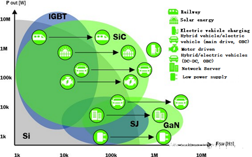
Gallium Nitride and Silicon Carbide devices, compete with silicon semiconductor (LDMOS) MOSFETs and superjunction MOSFETs.GaN and SiC devices are similar in some respects, but there are significant differences.

Figure 1. High voltage, high current, switching frequency relationship, and major application areas.
Wide-Band-Gap Semiconductors
WBG compound semiconductors have higher electron mobility and higher bandgap energy, which translates into superior characteristics to silicon. Transistors made from WBG compound semiconductors have higher breakdown voltage and tolerance to high temperatures. These devices offer advantages over silicon in high-voltage and high-power applications.

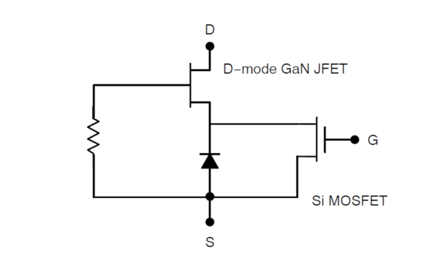
Figure 2. Dual die dual field effect tube (FET) cascade circuit converts GaN transistors into normally-off devices, enabling a standard enhanced mode of operation in high-power switching circuits
WBG transistors also switch faster and can operate at higher frequencies than silicon. Lower “on” resistance means they dissipate less power, resulting in improved energy efficiency. This unique combination of characteristics makes these devices attractive for some of the most demanding circuits in automotive applications, especially hybrid and electric vehicles.
GaN and SiC Transistors to Meet the Challenges of Automotive Electrical Devices
Key benefits of GaN and SiC devices: High voltage capability, with 650 V, 900 V and 1200 V devices available
Silicon Carbide:
Higher 1700V. 3300V and 6500V.
Faster switching speeds, higher operating temperatures.
Lower on-resistance, minimized power dissipation and higher energy efficiency.
GaN Devices
In switching applications, enhancement (or E-type) devices, which are usually “off”, are preferred, leading to the development of E-type GaN devices. This led to the development of E-type GaN devices, starting with a cascade of two FETs (Figure 2). Now, standard e-type GaN devices are available. They can be switched at frequencies up to 10 MHz with tens of kilowatts of power.
GaN devices are widely used in wireless devices as power amplifiers at frequencies up to 100 GHz. Some major use cases are cellular base station power amplifiers, military radar, satellite transmitters, and general purpose RF amplification. However, due to high voltage (up to 1,000 V), high temperature, and fast switching, they are also incorporated into a variety of switching power supply applications such as DC-DC converters, inverters, and battery chargers.
SiC Devices
SiC transistors are natural E-type MOSFETs. these devices can switch at frequencies up to 1 MHz with much higher voltage and current levels than silicon MOSFETs. maximum drain-source voltages are up to about 1,800 V with a current capability of 100 amps. In addition, SiC devices have much lower on-resistance than silicon MOSFETs, resulting in higher energy efficiency in all switching-mode power supply applications (SMPS designs).
SiC devices require a gate voltage drive of 18 to 20 volts to conduct devices with low on-resistance. Standard Si MOSFETs require less than 10 volts at the gate for full conduction. In addition, SiC devices require a gate drive of -3 to -5 V to switch to the off state.The ability of SiC MOSFETs to operate at high voltage and high current makes them well suited for use in automotive power circuits.
In many applications, IGBTs are being replaced by SiC devices.SiC devices can switch at higher frequencies, which reduces the size and cost of inductors or transformers while improving energy efficiency. In addition, SiC can handle higher currents than GaN.
GaN and SiC devices compete, especially silicon LDMOS MOSFETs, superjunction MOSFETs, and IGBTs. are being gradually replaced by GaN and SiC transistors in many applications.
To summarize GaN vs. SiC, here are the highlights:
GaN switches faster than Si.
SiC operates at a higher voltage than GaN.
SiC requires a high gate drive voltage.
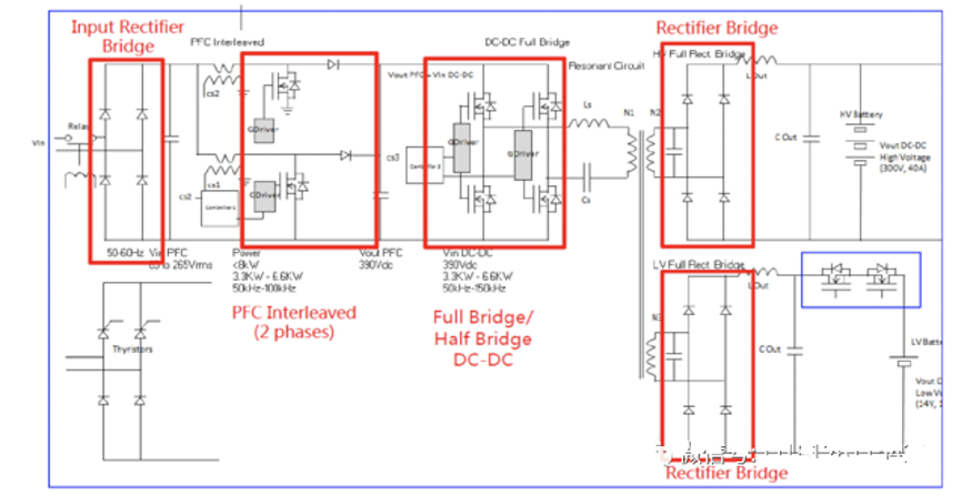
Many power circuits and devices can be improved by designing with GaN and SiC. One of the biggest beneficiaries is automotive electrical systems. Modern hybrids and pure electric vehicles contain equipment that can use these devices. Some of the popular applications are OBCs, DC-DC converters, motor drivers, and laser radar (LiDAR). Figure 3 points out the major subsystems in EVs that require high power switching transistors.

Fig. 3. WBG on-board charger (OBC) for hybrid and electric vehicles. The AC input is rectified, power factor corrected (PFC), and then DC-DC converted (one output is used to charge the high-voltage battery and the other is used to charge the low-voltage battery).
DC-DC converter. This is a power supply circuit that converts the high battery voltage to a lower voltage to run other electrical devices. Batteries now range up to 600 volts or 900 volts. the DC-DC converter steps it down to 48 volts or 12 volts, or both, for the operation of other electronic components (Figure 3). In hybrid electric vehicles and electric vehicles (HEVEVs), DC-DC can also be used for the high-voltage bus between the battery pack and the inverter.
On-Board Chargers (OBCs). Plug-in HEVEVs and EVs include an internal battery charger that can be connected to an AC power source. This allows charging at home without the need for an external AC- DC charger (Figure 4).
Main Drive Motor Drive. The main drive motor is a high-output AC motor that drives the vehicle’s wheels. The driver is an inverter that converts battery voltage to three-phase AC power to run the motor.

Figure 4. A typical DC-DC converter is used to convert high battery voltage to 12 and/or 48 volts. The IGBTs used in high voltage bridges are gradually being replaced by SiC MOSFETs.
GaN and SiC transistors offer automotive electrical designers flexibility and simpler designs as well as superior performance due to their high voltage, high current and fast switching characteristics.
